How to convert a schematic to a pcb layout with pcb creator Smps fullbridge pfc schematic + pcb layout pdf Schematics raypcb convert
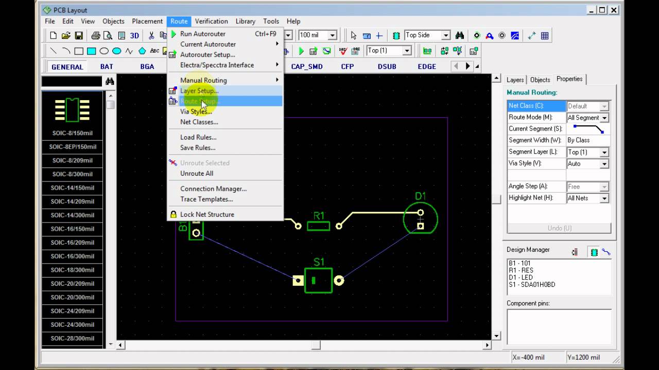
Free PCB Schematic Entry & Layout Software Beat Eagle for Some Features
Analog to digital converter circuit Pcb buck converter 5v 12v layout 3a thanks Boost converter pcb layout
Free pcb schematic entry & layout software beat eagle for some features
Pcb schematic make layout audio circuit custom amp startsPcb layout dc converter buck high density ti implementation synchronous power converters 25a part figure e2e components size blogs How to convert schematic diagram into pcb layout in easyeda online pcbAnalog circuit converter digital simple schematic diagram using pcb parts layout components sided actual copper single size projects clock fig.
High density pcb layout of dc/dc converters, part 2Pcb schematic creator layout convert Difference between schematic diagram and pcb layoutFrom idea to schematic to pcb.
Difference between schematic diagram and pcb layout : diptrace
Pcb schematic diagram layout easyeda convert into onlineSmps pcb pfc layout 4kva schematic fullbridge pdf circuit electronic tested ni Pcb schematic layout software eaglePcb schematic software layout expresspcb technical.
Pcb schematic easily idea doPcb design World technical: expresspcb schematic and pcb design software new versionHow to design a pcb layout.

Pcb boost converter eevblog forum
.
.


layout - 12V to 5V buck converter 3A PCB - Electrical Engineering Stack

world technical: ExpressPCB schematic and PCB design software new version

How to Design a PCB Layout - Circuit Basics

Free PCB Schematic Entry & Layout Software Beat Eagle for Some Features

From Idea to Schematic to PCB - How to do it easily! - YouTube

Difference Between Schematic Diagram And Pcb Layout : Diptrace

Difference Between Schematic Diagram And Pcb Layout - Points To Note

Boost Converter PCB Layout - Page 1

Analog To Digital Converter Circuit